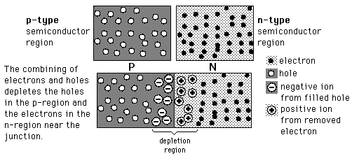
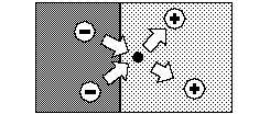
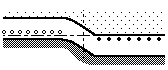
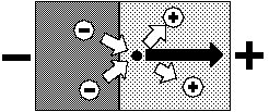
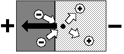
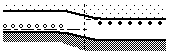
P-N Junction

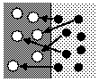
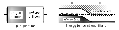
One of the crucial keys to solid state electronics is the nature of the P-N junction. When p-type and n-type materials are placed in contact with each other, the junction behaves very differently than either type of material alone. Specifically, current will flow readily in one direction (forward biased) but not in the other (reverse biased), creating the basic diode. This non-reversing behavior arises from the nature of the charge transport process in the two types of materials.

Index

Semiconductor concepts

Semiconductors for electronics
 
HyperPhysics***** Condensed Matter R Nave
Go Back


Depletion Region

When a p-n junction is formed, some of the free electrons in the n-region diffuse across the junction and combine with holes to form negative ions. In so doing they leave behind positive ions at the donor impurity sites.

Show more detail of depletion region.
Index

Semiconductor concepts

Semiconductors for electronics
 
HyperPhysics***** Condensed Matter R Nave
Go Back


Depletion Region Details

In the p-type region there are holes from the acceptor impurities and in the n-type region there are extra electrons.
When a p-n junction is formed, some of the electrons from the n-region which have reached the conduction band are free to diffuse across the junction and combine with holes.
Filling a hole makes a negative ion and leaves behind a positive ion on the n-side. A space charge builds up, creating a depletion region which inhibits any further electron transfer unless it is helped by putting a forward bias on the junction.
Show effects of biasing.
Index

Semiconductor concepts

Semiconductors for electronics
 
HyperPhysics***** Condensed Matter R Nave
Go Back


Bias effect on electrons in depletion zone

PN
Equilibrium ofjunction
Coulomb force from ions prevents further migration across the p-n junction.
PN
Reverse bias
Applied electric field further impedes the flow of electrons across the junction.
PN
Forward bias
Applied electric field assists electrons in overcoming the coulomb barrier of the space charge in depletion region.
Click on one of the junction conditions for more detail.
Index

Semiconductor concepts

Semiconductors for electronics
 
HyperPhysics***** Condensed Matter R Nave
Go Back