Intrinsic Semiconductor

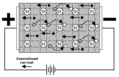
A silicon crystal is different from an insulator because at any temperature above absolute zero temperature, there is a finite probability that an electron in the lattice will be knocked loose from its position, leaving behind an electron deficiency called a "hole".
If a voltage is applied, then boththe electron and the hole can contribute to a small currentflow.

The conductivity of a semiconductor can be modeled in terms of the band theory of solids. The band model of a semiconductor suggests that at ordinary temperatures there is a finite possibility that electrons can reach the conduction band and contribute to electrical conduction.

The term intrinsic here distinguishes between the properties of pure "intrinsic" silicon and the dramaticallydifferent properties of doped n-type or p-type semiconductors.

Index

Semiconductor concepts
 
HyperPhysics***** Condensed Matter R Nave
Go Back


Semiconductor Current

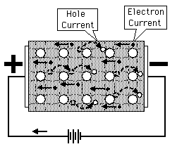
Both electrons and holes contribute to current flow in an intrinsic semiconductor.
Further discussion
Index

Semiconductor concepts
 
HyperPhysics***** Condensed Matter R Nave
Go Back


Semiconductor Current

The current which will flow in an intrinsic semiconductor consists of both electron and hole current. That is, the electrons which have been freed from their lattice positions into the conduction band can move through the material.
In addition, other electrons can hopbetween lattice positions to fillthe vacancies left by the freed electrons. This additional mechanismis called hole conduction becauseit is as if the holes are migrating across the materialin the direction opposite to the free electron movement.

Index

Semiconductor concepts
 
HyperPhysics***** Condensed Matter R Nave
Go Back


Electrons and Holes

In an intrinsic semiconductor like silicon at temperatures above absolute zero, there will be some electrons which are excited across the band gap into the conduction band and which can produce current. When the electron in pure silicon crosses the gap, it leaves behind an electron vacancy or "hole" in the regular silicon lattice. Under the influence of an external voltage, both the electron and the hole can move across the material. In an n-type semiconductor, the dopant contributes extra electrons, dramatically increasing the conductivity. In a p-type semiconductor, the dopant produces extra vacancies or holes, which likewise increase the conductivity. It is however the behavior of the p-n junction which is the key to the enormous variety of solid-state electronic devices.


Effective masses of electrons and holes
Index

Semiconductor concepts
 
HyperPhysics***** Condensed Matter R Nave
Go Back